Anatomy of a Hack assembly program - Part 1
This blog series is based on nand2tetris book.
I don’t have a comprehensive knowledge of hardware nor low-level programming. However, I have been learning this so long mistery part of computers since the last Summer. I will try to do my best to explain how a Hack assembly is translated into binary instructions and how the Hack machine does process a single instruction in a fetch and execute loop.
- First Part
- Second Part
I was always fascinated by how the operating system orchestrates all the components on a computer but I’ve never previously had the chance to learn the low-level details of this hidden world. Since last summer, I’ve started to explore and uncover the details of this beautiful yet complex landscape and I want to share what I learnt so far from the books I read.
The first book I started to read was the Elements of Computing Systems (AKA nand2tetris) which has amazing content that uncovers most of the topics I always wanted to learn. In order to reinforce what I learnt from the book, I decided to write about how a Hack assembly program flows through hardware. I will try to do my best to explain the details an emphasize on the parts that I think really crucial.
Before we dive into a Hack assembly program, let’s look into to specification of the Hack hardware platform.
The Hack Hardware Platform Specification
The Hack platform is a 16-bit von Neumann machine, designed to execute programs written in the Hack machine language. In order to do so, the Hack platform consists of a CPU, two separate memory modules serving as instruction memory and data memory, and two memory-mapped I/O devices: a screen and a keyboard.
The Hack CPU consists of the ALU and three registers called data register (D), address register (A), and program counter (PC). While the D-register is used solely for storing data values, the A-register serves three different purposes, depending on the context in which it is used: storing a data value (just like the D-register), pointing at an address in the instruction memory, or pointing at an address in the data memory.
CPU - Parts
In order to implement the Hack CPU, we need an ALU chip capable of computing arithmetic/logical functions, a set of registers, a program counter, and some additional gates (Control Unit) designed to help decode, execute, and fetch instructions.
ALU (Arithmetic Logic Unit)
This is the part where actual processing (or the magic) happens. The Hack ALU computes a fixed set of functions out = fi(x, y) where x and y are the chip’s two 16-bit inputs, out is the chip’s 16-bit output, and fi is an arithmetic or logical function selected from 18 possible functions. We instruct the ALU which function to compute by setting six input bits, called control bits. The ALU can potentially compute 64 (2^6) different functions.
Two’s complement is used as the method of signed number representation. It allows computing of operations such as x-1 with ease: When zy and ny bits are 1, the y input is first zeroed, and then negated bit-wise. Bit-wise negation of zero gives the 2’s complement binary value of -1.
Specification
Chip name: ALU

Inputs:    x[16], y[16],                    // Two 16-bit data inputs
           zx,                              // Zero the x input
           nx,                              // Negate the x input
           zy,                              // Zero the y input
           ny,                              // Negate the y input
           f,                               // Function code: 1 for Add, 0 for And
           no                               // Negate the out output

Outputs:   out[16],                         // 16-bit output
           zr,                              // True iff out=0
           ng                               // True iff out<0

Function:  if zx then x = 0                 // 16-bit zero constant
           if nx then x = !x                // Bit-wise negation
           if zy then y = 0                 // 16-bit zero constant
           if ny then y = !y                // Bit-wise negation
           if f then out = x + y            // Integer 2's complement addition
                else out = x & y            // Bit-wise And
           if no then out = !out            // Bit-wise negation
           if out=0 then zr = 1 else zr = 0 // 16-bit eq. comparison
           if out<0 then ng = 1 else ng = 0 // 16-bit neg. comparison

Comment:   Overflow is neither detected nor handled.
The above specification gives a clear idea of the implementation of the ALU. We only need a 16-bit Adder chip and a couple of logic gates including 16-bit Multiplexor, 16-bit NOT, 16-bit AND, 8-way OR, OR, and NOT.
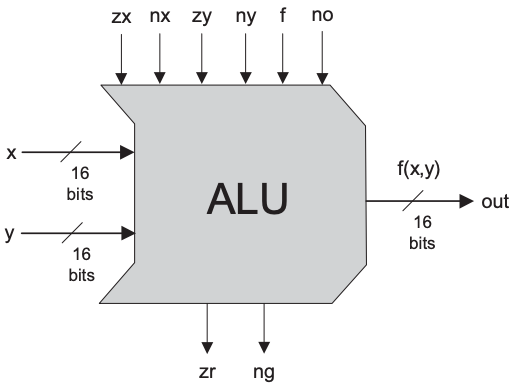
Figure 1: Arithmetic Logic Unit. (Taken from The Elements of Computing Systems, Chapter 2)
ALU computes one of the following instructions: x+y, x-y, y-x, 0, 1, -1, x, y, -x, -y, !x, !y, x+1, y+1, x-1, y-1, x&y, x|y on two 16-bit inputs, according to 6 input bits denoted by zx, nx, zy, ny, f, no. In addition, ALU computes two 1-bit outputs: if ALU output is 0 then zr is set to 1, otherwise zr is set to 0; if out<0 then ng is set to 1 otherwise ng is set to 0.
The below is an example implementation of the ALU in HDL (hardware description language).
// This file is part of www.nand2tetris.org
// and the book "The Elements of Computing Systems"
// by Nisan and Schocken, MIT Press.
// File name: projects/02/ALU.hdl

// Implementation: the ALU manipulates the x and y
// inputs and then operates on the resulting values,
// as follows:
// if (zx==1) set x = 0        // 16-bit constant
// if (nx==1) set x = ~x       // bitwise "not"
// if (zy==1) set y = 0        // 16-bit constant
// if (ny==1) set y = ~y       // bitwise "not"
// if (f==1)  set out = x + y  // integer 2's complement addition
// if (f==0)  set out = x & y  // bitwise "and"
// if (no==1) set out = ~out   // bitwise "not"
// if (out==0) set zr = 1
// if (out<0) set ng = 1

CHIP ALU {
    IN
        x[16], y[16],  // 16-bit inputs
        zx, // zero the x input
        nx, // negate the x input
        zy, // zero the y input
        ny, // negate the y input
        f,  // compute  out = x + y (if 1) or out = x & y (if 0)
        no; // negate the out output

    OUT
        out[16], // 16-bit output
        zr, // 1 if (out==0), 0 otherwise
        ng; // 1 if (out<0),  0 otherwise

    PARTS:

    // if (zx==1) set x = 0
    Mux16(a=x,b=false,sel=zx,out=zxout);

    // if (zy==1) set y = 0
    Mux16(a=y,b=false,sel=zy,out=zyout);

    // if (nx==1) set x = ~x
    // if (ny==1) set y = ~y
    Not16(in=zxout,out=notx);
    Not16(in=zyout,out=noty);
    Mux16(a=zxout,b=notx,sel=nx,out=nxout);
    Mux16(a=zyout,b=noty,sel=ny,out=nyout);

    // if (f==1)  set out = x + y
    // if (f==0)  set out = x & y
    Add16(a=nxout,b=nyout,out=addout);
    And16(a=nxout,b=nyout,out=andout);
    Mux16(a=andout,b=addout,sel=f,out=fout);

    // if (no==1) set out = ~out
    // 1 if (out<0),  0 otherwise
    Not16(in=fout,out=nfout);
    Mux16(a=fout,b=nfout,sel=no,out=out,out[0..7]=zr1,out[8..15]=zr2,out[15]=ng);

    // 1 if (out==0), 0 otherwise
    Or8Way(in=zr1,out=or1);
    Or8Way(in=zr2,out=or2);
    Or(a=or1,b=or2,out=or3);
    Not(in=or3,out=zr);
}
Registers
I am going to pass the specification and the implementation part for the registers since our subject is only about the computational part of the Hack platform. However, it is still useful to know about the types of registers that reside physically inside the CPU.
Data Register
Data Register holds the contents of the memory which are to be transferred from the immediate access storage to other components or vice versa.
Addressing Register
Addressing Register holds the memory address of data that needs to be accessed. When reading from memory, data addressed by addressing register is fed into the data register and then used by the CPU.
Program Counter (Instruction Pointer)
Program Counter holds the memory address of the next instruction that would be executed.
Control Unit
Control Unit controls the flow of data between the CPU and other components. It is contained within the CPU and reponsible for decoding the instructions, and figuring out which instruction to fetch and execute next.
CPU - Specification
Hack platform’s CPU is designed to execute 16-bit instructions according to the Hack machine language specification. The CPU should be connected to two separate memory modules: Instruction memory (ROM) and data memory (RAM).
Chip Name: CPU              // Central Processing Unit
Inputs:    inM[16],         // M value input (M = contents of RAM[A])
           instruction[16], // Instruction for execution
           reset            // Signals whether to restart the current
                            // program (reset=1) or continue executing
                            // the current program (reset=0)
Outputs:   outM[16],        // M value output
           writeM,          // Write to M?
           addressM[15],    // Address of M in data memory
           pc[15]           // Address of next instruction
The below figures shows the proposed CPU implementation. It does not show the control logic, except for inputs and outputs of control bits, labeled with a circled “c”.
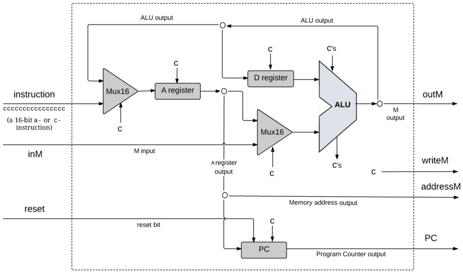
Figure 2: Central Processing Unit. (Taken from The Elements of Computing Systems, Chapter 5)
CPU executes the given instruction according to Hack assembly language specification. D and A refer to CPU-resident registers while M refers to external memory location addressed by A, i.e. to RAM[A]. inM holds the value of this location. If the current instruction needs to write a value to M, the value is placed in outM, the address of the target location is placed in the addressM output, and the writeM control bit is asserted.
outM and writeM outputs are combinational: they are affected instantaneously by the execution of the current instruction. addressM and pc outputs are clocked, they commit to their new values only in the next time unit. If reset=1 then the CPU jumps to address 0 (i.e. sets pc to 0 in next time unit) rather than to the address resulting from executing the current instruction.
This is an example implementation of the CPU in HDL:
// This file is part of www.nand2tetris.org
// and the book "The Elements of Computing Systems"
// by Nisan and Schocken, MIT Press.
// File name: projects/05/CPU.hdl

CHIP CPU {

    IN  inM[16],         // M value input  (M = contents of RAM[A])
        instruction[16], // Instruction for execution
        reset;           // Signals whether to re-start the current
                         // program (reset=1) or continue executing
                         // the current program (reset=0).

    OUT outM[16],        // M value output
        writeM,          // Write into M?
        addressM[15],    // Address in data memory (of M)
        pc[15];          // address of next instruction

    PARTS:
    Mux16(a=instruction,b=ALUout,sel=instruction[15],out=Ain);

    Not(in=instruction[15],out=notinstruction);

    //RegisterA
    //when instruction[15] = 0, it is @value means A should load value
    Or(a=notinstruction,b=instruction[5],out=loadA);//d1
    ARegister(in=Ain,load=loadA,out=Aout,out[0..14]=addressM);

    Mux16(a=Aout,b=inM,sel=instruction[12],out=AMout);

    //Prepare for ALU, if it is not an instruction, just return D
    And(a=instruction[11],b=instruction[15],out=zx);//c1
    And(a=instruction[10],b=instruction[15],out=nx);//c2
    Or(a=instruction[9],b=notinstruction,out=zy);//c3
    Or(a=instruction[8],b=notinstruction,out=ny);//c4
    And(a=instruction[7],b=instruction[15],out=f);//c5
    And(a=instruction[6],b=instruction[15],out=no);//c6

    ALU(x=Dout,y=AMout,zx=zx,nx=nx,zy=zy,ny=ny,f=f,no=no,out=outM,out=ALUout,zr=zero,ng=neg);

    //when it is an instruction, write M
    And(a=instruction[15],b=instruction[3],out=writeM);//d3

    //RegisterD,when it is an instruction, load D
    And(a=instruction[15],b=instruction[4],out=loadD);//d2
    DRegister(in=ALUout,load=loadD,out=Dout);

    //Prepare for jump
    //get positive
    Or(a=zero,b=neg,out=notpos);
    Not(in=notpos,out=pos);

    And(a=instruction[0],b=pos,out=j3);//j3
    And(a=instruction[1],b=zero,out=j2);//j2
    And(a=instruction[2],b=neg,out=j1);//j1

    Or(a=j1,b=j2,out=j12);
    Or(a=j12,b=j3,out=j123);

    And(a=j123,b=instruction[15],out=jump);

    //when jump,load Aout
    PC(in=Aout,load=jump,reset=reset,inc=true,out[0..14]=pc);
}
That’s it for the first part! We’ve done a great job so far and I know it was super overwhelming but all of the above information were necessary to understand how the binary instructions flow through the control unit. In the next part I will explain the Hack assembly language and how its instructions are translated into binary.